Bootable SPI flash
Introduction
All currently known Allwinner SoCs can boot from SPI flash, which usually has the lowest boot priority and is probed only after all the other options fail (SD card, NAND and eMMC).
Information for devboard designers
The SPI flash can be used to store a bootable firmware on the low cost development boards, which do not offer any other kind of non-removable storage (NAND or eMMC).
The minimum amount of the required storage would be 1 MiB (8 Mbit) to fit a user friendly bootloader with some advanced features. The prices of suitable SPI NOR flash chips seem to be around 10-20 cents on AliExpress (or even as low as only 4 cents?). This is non-negligible, but might be still worth it at least to avoid the frustrated "I plugged the power but there is nothing on the monitor" support requests from inexperienced users.
There is no point using SPI NOR flash chips larger than 16 MiB (128 Mbit). The primary use for this additional space would be a storage of some size reduced Linux kernel together with a small Buildroot generated compressed initrd image. And if no operating system is found on the SD card, then this built-in kernel+initrd can be booted instead. The whole point of having a kernel+initrd bundle in addition to just a bootloader is that developing the initrd is relatively easy, because it can be implemented using scripting languages and rely on existing GUI toolkits (Qt, FLTK, ...) or offer a text based user interface (via dialog or something similar). As for the provided functionality, it can do some hardware diagnostic self-tests and even update itself over Internet. In order to have a realistic size estimate, we can look at the kernel+intrd used for lima-memtester and see that it's size is less than 7 MiB, which would fit even into a 8 MiB (64 Mbit) SPI NOR flash chip. So it's a tight fit with 8 MiB (64 Mbit) and a lot of headroom with 16 MiB (128 Mbit). And an additional factor to consider is that programming NOR flash is slow and maxes at around ~200 KiB/s, so having smaller firmware reduces the time needed for flashing.
U-Boot can run UEFI applications since the release v2016.05, such as Grub2 or anything else. This is very nice, because it may provide a middle ground solution in terms of the firmware size (not as easy to implement as the kernel+initrd, but at least better than native U-Boot application hacks). There are some UEFI ports of the scripting language interpreters already available, such as Python/Lua and Ruby (Ssvb's favorite). But it is still not quite clear what is the UEFI GUI toolkits story.
The SPI flash chip needs to be connected to SPI0 pins (port C), which are multiplexed with NAND. There are also HOLD and WP pins, which need to be pulled up and optionally connected to the SoC GPIO pins for implementing write protect control in software. The table below lists the exact pins for different SoC variants and some additional notes:
| SoC name | SPI0 pins (MOSI,MISO,CLK,CS) | Total number of SPI controllers | Available SPI controllers if SPI flash is used | Possible implications of using SPI flash | Notes |
|---|---|---|---|---|---|
| A10/A20 | PC0,PC1,PC2,PC23 | 4 | 4 | Nothing significant. | SPI0 is also available on pins PI12,PI13,PI11,PI10 and can be used for other purposes even if a bootable SPI flash is hooked to PC0,PC1,PC2,PC23. |
| A13 | PC0,PC1,PC2,PC3 | 3 | 2 | Only one NAND chip can be used. | The SPI0_CS0 pin is multiplexed with NCE1 (the CS pin of the second NAND). |
| H3/H5 | PC0,PC1,PC2,PC3 | 2 | 1 | Only one NAND chip can be used. The only remaining free SPI1 controller is multiplexed with UART3 on pins PA15,PA16,PA14,PA13. | The SPI0_CS pin is multiplexed with NAND_CE1 (the CS pin of the second NAND). |
| A64 | PC0,PC1,PC2,PC3 | 2 | 1 | Only one NAND chip can be used. The only remaining free SPI1 controller is multiplexed with LCD and CCIR (camera?) on pins PD2,PD3,PD1,PD0 and this may be a problem. | The SPI0_CS pin is multiplexed with NAND_CE1 (the CS pin of the second NAND). |
It looks like SPI is getting gradually phased out from the newer Allwinner SoCs. This may be a problem for providing the necessary SPI pins for the Raspberry Pi compatible expansion headers or OLIMEX UEXT connectors.
The BROM implementation details
For SPI NOR flash booting, the BROM sets up 6 MHz (OSC24M with divisor 4?) clock frequency for SPI0 and then issues a sequence of Read Data Bytes (03h) commands. Each of these commands is encoded in 4 bytes (1 byte for the command id and 3 bytes for the address). The first command reads 256 bytes from the address 0. If a valid eGON header is recognized, then a sequence of commands reading 2048 byte blocks is done next. The first 2048 byte block is read from the address 0, the second 2048 byte block is read from the address 2048 and this continues until the whole first stage bootloader is transferred.
Some SoCs can also boot from SPI NAND flash. Here the BROM tries to read a valid first stage bootloader starting from page number 0, 32, 64, 96, 128, 160, 192 and 224. It only reads the first 1024 bytes from every page. Since it simply sends the standard SPI NAND flash commands, it is a good idea to use a flash with ECC turned on by default and is performed by the flash itself, since errors cannot otherwise be corrected.
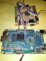
As an experiment, it is possible to configure SPI on one board in the slave mode, connect jumper wires and emulate the SPI flash for the BROM in another board. But the timing constraints are too tight to do a perfect emulation. A perfect emulation would need to correctly handle the Read Data Bytes command, which means that after the last bit of the address is received, the first bit of data from that address needs to be served back in the next SPI cycle. With such a protocol, we can't benefit from any kind of receive and transmit buffering and make use of the hardware SPI controller. For the GPIO bit-banging implementation of the 6 MHz SPI, we have around ~170 cycles per SPI bit at the 1008 MHz CPU clock frequency. This time is comparable to the DRAM access latency, so we are in a big trouble if we get any L2 cache misses (though this can be mitigated by prefetching the right cache line after receiving just enough of the address bits). Moreover, the GPIO itself is relatively slow and it takes a huge amount of CPU cycles to read/write GPIO registers. So a simplistic approach is just to use the SPI controller hardware, ignore any received commands and stream the data according to the expected pattern. That would be 4 padding bytes, then 256 initial bytes of the firmware, then 4 bytes padding again and 2048 initial bytes of the firmware, etc. And this works, see the picture on the right side :-)
Such SPI flash emulation using another board probably does not make much practical sense because it is possible to just connect a real SPI flash chip to the SPI pins. This was only a method get some information about the BROM behaviour. A more complete SPI flash emulation might be an interesting exercise to be done using the upcoming iCE40HX1K-EVB open source hardware FPGA board from OLIMEX.
Software development and trying something here and now
| This section is a bit out of date because the Xunlong Orange Pi PC 2 board is now available and it has built-in SPI flash. Some other boards are also underway and are expected to become available soon. |
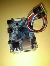
While there are no known boards with built-in SPI flash, it is still possible to arrange some test setup. The SPI0 pins are often available on the expansion headers. The picture on the right side shows how the SPI0_CS,SPI0_CLK,SPI0_MOSI,SPI0_MISO,3V3,GND pins on the Xunlong Orange Pi PC expansion header are connected to the CS,CLK,DI,DO,VCC,GND pins on the W25Q SPI flash module. The wires are entangled and tied in a knot, with the SPI flash module being more or less fixated in place and sticking upwards. Not a very aesthetically pleasing sight, but it works fine for testing the software.
The availability of the SPI0 (port C) pins on the expansion headers is both a blessing and a curse for the existing development boards, such as Xunlong Orange Pi PC and Pine64:
- On one hand, we can connect an SPI flash module to these pins using jumper wires and use this for prototyping and debugging code. Also some vendor may start making and selling nice factory-made SPI flash shields for the Raspberry Pi compatible expansion header.
- On the other hand, adding on-board SPI flash in the next revision of the same development board may be problematic because this can break compatibility with the existing shields and the software already developed for them. The device tree does not seem to be good enough (please correct this statement if it is wrong) and has no concept of describing standard GPIO expansion headers with full flexibility of transparently remapping pins in different board revisions. For example, replacing SPI0 pins with SPI1 pins on the 40pin Raspberry Pi compatible expansion header and describing this change only in one place in the board-specific DTS file (so that no changes are necessary in any shield-specific device tree overlays or in the userland software).
U-Boot support
| SoC name | SoC support status in U-Boot |
|---|---|
| A10 | Supported since v2016.09. But still untested because SPI0 is not easily accessible on popular boards. The test has been done only using a SPI2 based modification. |
| A13 / A20 A64 / H3 | Supported since v2016.09 |
| H5 | WIP |
The SPL
Current status
The basic SPI boot support is available since v2016.09 release. Note that booting from SPI flash is currently disabled by default and it is necessary to add one line to the board defconfig in order to use it:
CONFIG_SPL_SPI_SUNXI=y
In principle, enabling SPI flash support by default on every sunxi board should have no negative consequences for any other use cases, because this code only gets activated when the SPL part has been booted from SPI (by looking at the byte at the offset 0x28 in the SPL header). The only potential concern is the code size, which gets increased by ~370 bytes.
Future improvements
Taking care of the ATF and the AR100 firmware may need some additional tricks on AArch64 (packing multiple blobs in a FIT container? or use something more lightweight?). Though this is not really SPI boot specific.
Running SPI at only 6 MHz might be not fast enough and adding something like ~0.5 second to the boot time (needed to transfer ~500KB of the main U-Boot binary). In order to improve boot time a little bit, probably the SPL header can be extended to include a special optional field for the maximum supported SPI clock speed and also the number of dummy cycles for the Read Data Bytes at Higher Speed (0Bh) command. This information can be added to the SPL header by the firmware flasher software (see the "Upgrading the SPI flash firmware" section).
The main U-Boot binary
The main U-Boot binary can get a more complete implementation for handling SPI flash, also with a full write support by making use of the driver model and the existing SPI framework. However please also see the "Security considerations" section below, because it might be unreasonable to allow accessing the SPI flash from U-Boot in the case if U-Boot runs in the non-secure mode on AArch64. Either way, the SPI flash support in the main U-Boot binary is very much optional.
SPI driver
A driver model compatible SPI driver for u-boot was worked on and is now available in mainline u-boot (see below). In combination with the earlier work on the SPL, this driver allows for booting both u-boot and Linux from SPI flash. At the moment, the following boards have been tested:
- H2+ Orange Pi Zero with Macronix MX25L1605D 16 Mbit
- A20 OLinuXino LIME 2 with Winbond W25Q128BV 128 Mbit (booting FIT image from SPI flash)
- A64 Pine64+ with Winbond W25Q128BV 128 Mbit (using apritzel's sunxi64-beta64 branch)
- A64 OLinuXino with Eon EN25Q64 64 Mbit (using apritzel's sunxi64-beta64 branch)
Commits are available that modify the configs and device trees for these boards to enable full support by default.
After the u-boot binary has been built, it can be run on the board using the sunxi-fel tool or by programming the SPI flash chip. To load and boot a FIT image stored at 0x100000, the following sequence of commands can be used (assuming the size of the image is 0x400000):
   sf probe 0:0 6000000
   sf read 42000000 100000 400000
   bootm 0x42000000
The flash chip can also be erased and modified from within u-boot.
If you are trying to boot u-boot SPL from SPI flash directly on an Allwinner A10/A20 board, then make sure to power it using USB Y or AC. When the USB OTG cable is attached to a computer to power the board, it won't boot.
Mainline u-boot
A SPI flash driver is now available in mainline u-boot:
https://git.denx.de/?p=u-boot.git;a=commit;h=7f25d8179776226a8ecfbaad3d3a88e9acd89f28
You will need to enable CONFIG_SPI, CONFIG_SUN4I_SPI, CONFIG_CMD_SF, CONFIG_CMD_SSPI, CONFIG_DM_SPI, CONFIG_DM_SPI_FLASH, CONFIG_SPI_FLASH and optionally CONFIG_SPI_FLASH_MACRONIX and CONFIG_SPI_FLASH_WINBOND.
The device tree of the device will also need to be modified; see the various dts commits here: https://github.com/StephanvanSchaik/u-boot/commits/sunxi-spi
Reliability considerations
The SPI NOR flash chips are typically rated for 100000 erase cycles and 20 years of data retention. Also they have much lower data density than NAND and are sold without bad blocks. Still it is an open question whether any bad blocks may appear over time on some fraction of devices (if anyone has any relevant references, please add them here).
As a way to mitigate the risks, it may be possible to write a small bootable stub into the first 4096 byte sector on the SPI flash. The smallest possible size reduces the chances of it being damaged, also it does not need to be updated nearly as frequently as U-Boot. Right after this stub, there can be two copies of the regular U-Boot SPL. The bootable stub can then do the checksum verification and pick a non-damaged SPL copy (if one of them goes bad). As an additional bonus, such stub can support 40 KiB size for the SPL, thus overcoming the BROM limitation. As for the main U-Boot binary, storing two copies would waste too much space. But having CRC32 protected data blocks and an extra parity block can make it more damage resistant.
A rather old, but interesting post in the linux-mtd mailing list explained how the NOR flash wears out. Presumably it takes time for the unreliable bit to flip from 0 to 1, so this has some implications on the verification stage after the firmware had been programmed (do we need an extra delay there?).
Security considerations
It's a good idea to prevent unauthorized update of the firmware code (search for "BIOS trojan" keywords on google for more information on this topic). A malicious software trying to gain even more control over the system after exploiting one of the privilege escalation bugs in Linux could try a few tricks, listed in the table below.
| A possible attack vector | Risk mitigation |
|---|---|
| Program the SPI flash using the SPI0 controller. | There are some secure/non-secure peripheral access configuration knobs in the newer SoC variants, which can be investigated. Still untested and needs to be confirmed. |
| Program the SPI flash using simple GPIO bit-banging. | There are some secure/non-secure peripheral access configuration knobs in the newer SoC variants, which can be investigated. If restricting non-secure access to a single SPI CS pin is not possible on the GPIO port C, then the HOLD pin or the WP pin could be connected to one of the pins on the port L and asserted by the firmware. The whole port L can be then configured as secure only. Still untested and needs to be confirmed. |
| Write its own bootloader to some accessible higher priority bootable media (for example an SD card) and then program the SPI flash from it. | Some SoCs have special pins to configure the default boot order (the UBOOT_SEL pins in A31). The other SoCs could probably use MMC1 instead of MMC0 for the SD card slot to ensure that the firmware always boots for the SPI flash. Still untested and needs to be confirmed. |
Ideally, the user should have full control over the firmware upgrade (it is the user who owns the device and not the other way around). When having physical assess to the device, the firmware is always upgradable from the FEL mode (which is activated by pressing a hardware FEL button). And for the sake of convenience, when doing upgrades on the device itself, the firmware can implement asymmetric cryptography to ensure that upgrade only happens to new versions of the firmware from the same trusted author.
Upgrading the SPI flash firmware
Multiple methods could be potentially used:
- For dealing with completely bricked non-bootable boards, the most simple solution would be probably to use the sunxi-fel tool with an added feature to backup and flash the firmware.
- For additional users convenience, it would be nice to support upgrading the firmware from the running system too.
Using the sunxi-fel tool
The sunxi-fel tool can be run on an x86 desktop system to program the SPI flash over a Micro-USB cable and bring a non-bootable Allwinner device back to life [1]. Just upgrading or initially programming the SPI flash firmware on a perfectly working device is possible too.
Trying to check if there is a real SPI flash chip connected to SPI0 pins (after connecting some Allwinner device to your desktop PC via a Micro-USB cable and booting the device in FEL mode):
./sunxi-fel spiflash-info
Programming a compiled U-Boot image to the SPI flash:
./sunxi-fel -p spiflash-write 0 u-boot-sunxi-with-spl.bin
Checking if flash programming has been successful:
   ./sunxi-fel -p spiflash-read 0 `stat -c %s u-boot-sunxi-with-spl.bin` spi-flash-read-data.bin
   cmp -b u-boot-sunxi-with-spl.bin spi-flash-read-data.bin
After this, the U-Boot bootloader should be successfully getting booted from the SPI flash after rebooting the device (assuming that no higher priority boot media is available).
- ↑ Assuming that the device has an SPI flash chip connected to SPI0 and boots from it in the first place, which is usually not the case except for Xunlong Orange Pi PC 2 and probably ViPER MovieMate.
Using the flashrom tool from a running Linux system on the device
In order to be able to access the SPI flash from Linux, it is necessary to have some device tree nodes describing this hardware. There are two possible ways to do this:
- Have the SPI0 bus described as a generic spidev node.
- Have the exact SPI flash chip description in the device tree.
Both of these approaches are technically correct. But from the ideological point of view, the latter solution is required. One more difficulty is that the SPI flash is multiplexed with NAND and this also needs to be addressed properly. Rather than editing DTS files all the time (especially if the SPI flash is hooked to the expansion header), this information can be added to the device tree on the fly by the U-Boot bootloader.
As for the sunxi SPI driver in the mainline kernel, it is currently in a rather bad shape and does not support sending/receiving SPI messages larger than the FIFO size. Since the FIFO size is only 64 bytes and programming the SPI flash is normally done as 256 byte pages, such limitation most likely renders the SPI driver unusable for this particular use case (to be confirmed). There is some ongoing work, trying to address the sunxi SPI driver problems in the mainline kernel:
- http://lkml.iu.edu/hypermail/linux/kernel/1404.0/00647.html
- http://lists.infradead.org/pipermail/linux-arm-kernel/2014-June/263745.html
- https://www.marc.info/?l=linux-arm-kernel&m=146584014828666&w=3
None of these tasks is particularly challenging from the purely technical point of view, but kernel bureaucrats may turn this activity into a long lasting open source show...
Using some special firmware upgrade interface
The firmware may try to expose a simple interface for upgrading itself. It also may make use of a digital signature check and other safety measures. We need to find out if there are any standard interfaces of this kind already specified for AArch32/AArch64 hardware. The https://github.com/ARM-software/arm-trusted-firmware/blob/master/docs/firmware-update.md page may be a good start.
Before using the firmware upgrade interface, the kernel should temporarily stop using SPI0 and/or NAND. And also preferably temporarily release the SPI0/NAND pins, so that the firmware can confirm this fact itself. The HOLD or WP pin can be used for enabling/disabling access to the SPI flash hardware. And this pin should be preferably accessible only from the firmware, but not from the kernel (of course this is only relevant if we do care about security).
Please note that even if the firmware upgrade fails (or is not implemented at all), it is always possible to use the sunxi-fel tool.
The list of known SPI flash chips
The Read JEDEC ID (9Fh) command is supposed to be around since 2003. The Read SFDP command is relatively new and is documented in the JEDEC standard JESD216, published on 2011. The updated JESD216B standard from 2013 also describes how to use capacities larger than 128 Mbit in a generic way (such capacities exceed the legacy 24-bit addressing mode and can't be used with the old commands).
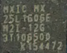
Macronix MX25L1606E
This is a 16 Mbit chip, which is used by the Xunlong Orange Pi PC 2 board. Supports the JEDEC ID (9Fh) command and returns the 0xC22015 id. Also supports the Read SFDP (0x5A) command and returns:
00000000: 53 46 44 50 00 01 01 ff 00 00 01 09 30 00 00 ff  SFDP........0...
00000010: c2 00 01 04 60 00 00 ff ff ff ff ff ff ff ff ff  ....`...........
00000020: ff ff ff ff ff ff ff ff ff ff ff ff ff ff ff ff  ................
00000030: e5 20 81 ff ff ff ff 00 00 ff 00 ff 08 3b 00 ff  . ...........;..
00000040: ee ff ff ff ff ff 00 ff ff ff 00 ff 0c 20 10 d8  ............. ..
00000050: 00 ff 00 ff ff ff ff ff ff ff ff ff ff ff ff ff  ................
00000060: 00 36 00 27 f6 4f ff ff fe cf ff ff ff ff ff ff  .6.'.O..........
00000070: ff ff ff ff ff ff ff ff ff ff ff ff ff ff ff ff  ................
Based on the information from the datasheet, the Typical Page Program Time (256 bytes) is 0.6 ms and the Typical Block Erase Time (64 KiB) is 400 ms. Simple calculations show that the expected flashing speed would be
1 / (0.6 ms / 256 bytes + 400 ms / 65536 bytes) = ~118 kB/s.
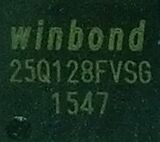
Winbond 25Q128FVSG
This is a 128 Mbit chip, which is used by the SOPINE A64 compute module. Supports the JEDEC ID (9Fh) command and returns the 0xEF4018 id. Also supports the Read SFDP (0x5A) command and returns:
00000000: 53 46 44 50 00 01 00 ff 00 00 01 09 80 00 00 ff  SFDP............
00000010: ff ff ff ff ff ff ff ff ff ff ff ff ff ff ff ff  ................
00000020: ff ff ff ff ff ff ff ff ff ff ff ff ff ff ff ff  ................
00000030: ff ff ff ff ff ff ff ff ff ff ff ff ff ff ff ff  ................
00000040: ff ff ff ff ff ff ff ff ff ff ff ff ff ff ff ff  ................
00000050: ff ff ff ff ff ff ff ff ff ff ff ff ff ff ff ff  ................
00000060: ff ff ff ff ff ff ff ff ff ff ff ff ff ff ff ff  ................
00000070: ff ff ff ff ff ff ff ff ff ff ff ff ff ff ff ff  ................
00000080: e5 20 f1 ff ff ff ff 07 44 eb 08 6b 08 3b 42 bb  . ......D..k.;B.
00000090: fe ff ff ff ff ff 00 00 ff ff 21 eb 0c 20 0f 52  ..........!.. .R
000000a0: 10 d8 00 00 ff ff ff ff ff ff ff ff ff ff ff ff  ................
000000b0: ff ff ff ff ff ff ff ff ff ff ff ff ff ff ff ff  ................
It is conforming to the old JESD216 standard. This old standard can only specify write granularity as either 1 byte or 64 bytes, while we want to use full 256 bytes page size for better performance. So it makes sense to identify this chip using the JEDEC ID (9Fh) command and use the retrieved id for a table lookup.
Based on the information from the datasheet, the Typical Page Program Time (256 bytes) is 0.7 ms and the Typical Block Erase Time (64 KiB) is 150 ms. Simple calculations show that the expected flashing speed would be
1 / (0.7 ms / 256 bytes + 150 ms / 65536 bytes) = ~199 kB/s.
Note that unlike the erasing/programming operation, reading speed is very fast for the NOR flash and is only limited by the SPI interface.
25Q128FV
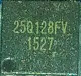
This is a noname 128 Mbit chip, which is used in W25Q SPI flash module from ebay. Supports the JEDEC ID (9Fh) command and returns the 0xEF4018 id (the same as the Winbond 25Q128FVSG). Does not support the Read SFDP (0x5A) command, but other than this seems to be pretty much compatible.
See also
- SPIdev
- Wikipedia on NOR flash
- Migrating from Winbond W25Q-FV, Micron N25Q-A, and Macronix M25L-F Devices to Cypress S25FL-L (useful for checking the SPI commands compatibility overview)
