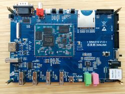
Sinlinx SinA31s
| Sinlinx SinA31s | |
|---|---|
 | |
| Manufacturer | Sinlinx |
| Dimensions | 170mm x 118mm |
| Release Date | August 2014 |
| Website | Device Product Page |
| Specifications | |
| SoC | A31s @ 1008Mhz |
| DRAM | 1GiB DDR3 @ 432MHz (2x Samsung K4B4G1646Q-HYK0) |
| NAND | 4 / 16 GB eMMC (Samsung KLMAG2GE4A-A001) |
| Power | DC 5V @ 2A, Battery connector solder points |
| Features | |
| LCD | 1024x600 (7" optional) |
| Touchscreen | X-finger capacitive (AWinic AW5206) on optional LCD |
| Video | HDMI (Type A - full), optional LCD-VGA converter |
| Audio | 3.5mm headphone plug, 3.5mm microphone plug, HDMI, SPDIF |
| Network | 10/100Mbps Ethernet (Realtek RTL8201CP) |
| Storage | µSD, eMMC |
| USB | 5 USB2.0 Host, 1 USB2.0 OTG |
| Other | IR |
| Headers | LCD, SDIO, CSI, USER IO |
The SinA31s is an A31s core/daughter board combo from Sinlinx. The core board can be purchased separately and integrated into other projects.
Identification
The PCB has the following silkscreened on it:
SINA31S 芯灵思 | SINLINX
In android, under Settings->About Tablet, you will find:
- Model Number: Allwinner-Tablet
- Build Number: fiber_a31st-eng 4.2.2 JDQ39 20140725 test-keys
Sunxi support
Current status
This board is supported on mainline U-Boot and Linux kernel. See sections below.
Manual build
You can build things for yourself by following our Manual build howto and by choosing from the configurations available below.
U-Boot
Mainline U-Boot
For building mainline u-boot, use the SinA31s target.
Mainline kernel
Use the sun6i-a31s-sina31s.dtb device-tree file for the mainline kernel.
Tips, Tricks, Caveats
FEL mode
The U-Boot button triggers booting from mmc0 directly, and falls back to FEL mode if that fails.
Core / Daughter Board
The SinA31s consists of a core board and a daughter board, or as the vendor calls them, a CPU board and an SDK board.
Core Board
The core board consists of the A31s SoC, AXP221s PMIC, DRAM, eMMC, and supporting components. There are at least 2 revisions, though there doesn't seem to be any significant changes.
There are 3 also empty pad groups, J1, J2, and J3. J1 has UART0 and JTAG pins. J2 has I2S0 pins. J3 has CPUS UART and JTAG pins.
SDK Daughter Board
The daughter board breaks out all the pads from the core board into useful peripherals. There are at least 2 revisions. One way to see if you have a newer board is to check whether the HDMI port has ESD protection components near it.
The SDK daughter board has many connectors, as can be seen from the pictures below. There are 4 expansion headers: LCD, Camera, SDIO, and USER IO. The first three are designed to work with modules from Sinlinx, though you may use other modules provided you swap around the cabling.
The USER IO header is different between older and newer revisions.
Optional LCD / VGA converter
Sinlinx provides a 7" LCD with capacitive touchscreen, or an LCD to VGA converter board, for video display.
7" LCD screen
To use the LCD with mainline U-boot, have the following config options set:
CONFIG_VIDEO_LCD_MODE="x:1024,y:600,depth:18,pclk_khz:66000,le:90,ri:160,up:3,lo:127,hs:70,vs:20,sync:3,vmode:0"
CONFIG_VIDEO_LCD_DCLK_PHASE=0
Serial console port
The SDK daughter board uses a converter chip to convert the UART signal level to RS232 levels. On the upper side of the board is a 9-pin RS232 connector.
You can also use the UART0 pads on the core board.
Pictures
See also
Manufacturer images
Sinlinx provides Android and Linux images to buyers, hosted on BaiduPan (Baidu's cloud storage).


