PocketBook Touch Lux 3
| PocketBook Touch Lux 3 | |
|---|---|
 | |
| Manufacturer | PocketBook |
| Dimensions | 114.6mm x 174.4mm x 8.3mm |
| Release Date | 2015? |
| Website | Device Product Page |
| Specifications | |
| SoC | A13 @ 1Ghz |
| DRAM | 256MiB DDR3 @ 408MHz |
| Power | USB 5V @ 0.5-1A, 1500mAh 3.7V Li-Ion battery |
| Features | |
| LCD | 1024x758 (6") |
| Touchscreen | multi-finger capacitive (Cypress TMA445 / fw 0x0108) |
| Video | proprietary eInk display / ED060XD4 |
| Audio | none |
| Network | WiFi 802.11 b/g/n (RTL8188EUS) over USB |
| Storage | 2x µSD (one internal, one external), SPI NOR |
| USB | 1x internal USB2.0 Host, 1x USB2.0 OTG (external, peripheral mode only) |
| Camera | none |
| Other | AXP209, TP65185 PMICs, pcf8563 RTC |
| Headers | UART |
Identification
On the back of the device, the following is printed:
PocketBook Touch Lux 3
The PCB has the following silkscreened on it:
IDIG E028 PB626 V1.6
20141229
PocketBook manufactured on 20/08/2018 has this silkscreened on the PCB
XRZ_E028 PB626-V2.1
20170406
Most notable change is usage of 8GB eMMC storage on the new board and Elan touch screen.
Sunxi support
Current status
- Full mainline/linux/u-boot support for all HW (with some extra out-of-tree patches), including a kernel driver for controlling the eInk display via DEBE/TCON0 with an ability to precisely time the ink manipulation down to multiples of 50ns. The driver can achieve full speed (85Hz) communication with the display. Interface is via writing a framebuffer to a special character device /dev/eink-panel.
TODO
- The display driver is now mature enough to allow for easy experimentation with the display.
- Instead of pushing all the complexity of parsing waveform data and figuring out what to do to move the ink from a current position to a new one to kernel space, the driver provides the base interface for writing a precisely timed frame to the display. Waveform parsing, temperature adjustment of timings, and choosing an algorithm to update different regions of the display is left to the userspace, where it can be much more easily experimented with and used to provide the best experience based on what content is displayed in what regions of the screen.
- Waveforms for the display are stored on the SPI NOR flash, analyze the format to see how the timings are specified.
- Waveforms can be read using https://github.com/fread-ink/inkwave, precise meaning of data stored therein is still unclear, though
- Re-check USB0, if perhaps it can support at least a forced host mode. (would need a VBUS switch)
- Reduce data copying by using memory mapped buffers. (this can save ~ 800us)
- Allow to interleave submission of a next buffer and processing of the current one (submission takes ~8ms with all the scheduling, copying and conversion of FB data to display control stream). This would allow for going from 50Hz update rate to ~100Hz
- Write a tool to manage transitions between different display states using NEON intrinsics.
Images
Pre-built kernel/u-boot available at https://xff.cz/kernels
BSP
- https://github.com/pocketbook/Platform_A13 (does not contain code for all drivers, code for cyttsp4.ko, epdc.ko is missing)
Manual build
You can build things for yourself by following our Manual build howto and by choosing from the configurations available below.
U-Boot
Sunxi/Legacy U-Boot
No u-boot code is available from the manufacturer.
Mainline U-Boot
Not yet upstreamed, but patches are available here for now:
Use the pocketbook_touch_lux_3_defconfig build target.
Linux Kernel
Mainline kernel
The board support is mostly upstreamed, except for touchscreen patches and the display support. Non-upstreamed changes are in this branch:
Use the sun5i-a13-pocketbook-touch-lux-3.dtb device-tree binary and pocketbook_touch_lux_3_defconfig config.
Tips, Tricks, Caveats
- You can buy any variant of ED060XD4 display for Touch Lux 3, replacement requires some care not to break anything. The display is glued to the plastic frame with an double-sided adhesive tape. It's possible to separate the display from the frame by sticking some flat sharp plastic tool between the display and the frame from the front side. I used an old credit card. The trick is to try to swipe the card along all edges of the display, while laying it mostly flat on the display. You can replace the display without glueing the new one in.
- There are three variants of the display available: just the eInk display (matte or gloss) (~$13-15), eInk+backlight (~$25), eInk+backlight+touch digitizer (~$50-65). Some manufacturers claim on Aliexpress that they provide the panels for PocketBook and that their displays are matte and have even backlight. I can confirm that. I also confirmed that using the cheapest $13 replacement display without backlight also works. (original firmware has trouble booting when touch panel digitizer is not detected, so using a cheap display is adviseable if you don't want to use the original firmware)
- After installing the new display, touchscreen may be acting weirdly. That may not mean it's broken, it may just need calibration. Calibration is performed by writing a bunch of values to bunch of registers. Nothing special. There's a confusingly named S06-xc4_calibrate.sh script in the original firmware's boot partition that can be used to do calibration with the original kernel. I plan to add support for calibration to the mainline driver.
- I doubt it's possible to replace backlight cable without breaking the connector. The connector is extremely fragile. I used thermal glue pistol to fix the new cable in place but it's still easy to cause shorts and shutdown the regulator, just by pressing device buttons or by pressing on the back cover. Thankfully the PMIC is resilient and will only shut down the backlight regulator if it detects the short-circuit. Regulator can be restarted by disabling/enabling the backlight in sysfs.
FEL mode
The Menu button on the right side triggers FEL mode.
List of HW
Reverse enginnered:
SoC: A13 rev b

DRAM: 256MiB (Samsung k4b2g1646q-bck0)

Internal uSD card slot (4-bit) (MMC2)
  - works out of the box

External uSD card slot (4-bit) (MMC0)
  - PE4 needs to be driven low to enable it
  - PG0 is connected to CD
  - can't boot

ED060XD4 display with touch panel and backlight
  + MX25U4033 512kB flash on the dispaly FFC (SPI)
  + Cypress TMA445 FW 0x0108 touch controller
  + TP65185 eInk voltage regulator

Serial debug port at PG3/PG4 3.3V (UART1)

I2C devices:

  I2C-0 (PB0/PB1)
    AXP209 @0x34 (CHIP ID: 0x41)
      LDO1 1.3V (1.3V)
      LDO2 3V  (1.8-3.3V)
      LDO3 3.3V (0.7-3.5V)   - powers wifi chip (needs slew rate control on enable)
      LDO4 3.3V (1.2-3.3V)
      BUCK2 1.4V  (0.7-2.275V)
      BUCK3 1.2V  (0.7-3.5V)
      LDOIO0 1.8V (1.8V)

      - POK key input

  I2C-1 (PB15/PB16)
    - RTC / pcf8563 @0x51
    - TP65185 @0x68
      - NCP18XH103F03RB NTC thermistor connected on the FFC

  I2C-2 (PB17/PB18)
    - Cypress TMA445 @0x24
      - Power 1.8V
        - Enabled by PC15=1 and PC13=1

SPI devices:

  SPI-2 (PE0-PE3)
    - MX25U4033
      - Power 1.8V
        - enabled by PC15=1 and PC14=1
      - PE1 kills usb bus?

Backlight via PWM:
  - enable at PB4
  - pwm at PB2

GPIO buttons:
  - at PG9 and PG10

Power LED:
  - at PE8

USB:
  - host controller connected to the USB wifi chip

WiFi:
  - RTL8188EUS 802.11n Wireless Network Adapter
  - 0x0bda:0x8179
  - CHIP_8188E_Normal_Chip_TSMC_UNKNOWN_CUT(10)_1T1R_RomVer(0)
  - EEPROM ID=0x8129

USB OTG:
  - only peripheral mode, as ID detection pin is not routed to SoC
    - id-det from fex should be at PG2, but does not react to plug-in
  - vbus is not controllable
    - detection should be at PG1 (not tested)
    - vbus enable shoudld be at PG12 (not working)
Also see DTS file, wich contains more details.
ED060XD4 eInk display
This display is sold in 3 variants on the internet. Just eInk display panel, + backlight, + backlight and touch.
Current status of reverse engineering:
FFP pinout: (reverse engieneered)
---------------------------------
It turns out that ED060XD4 has the same interface as ED060XC5 or ED060XC3 (Touch Lux 2).

The datasheet for ED060XC5 is available on the internet. It looks like ED060XG1 has also
the same interface and its datasheet contains extra timing/interface
information, that can be useful.

FFP pin | SoC   | Meaning              | Open questions?
--------|-------|----------------------|---------------------
1       |       | 22V                  |
2       |       | 15V                  |
3       |       | GND                  |
4       |       | BORDER               | Thin wire to the panel (border voltage)
5       |       | Flash VCC 1.8V       | PC14 and PC15 are set (thicker wire)
6       | D23   | GA START PULSE - SPV | somehow special (set to 1 when not transmitting)
7       | D22   | GA CLK - CKV         |
8       | D15   | MODE 1               |
9       |       | GND                  |
10      | PE3   | Flash SO             |
-------------------------------------------------------------
11      | PE0   | Flash CS#            |
12      | PE2   | Flash SI             |
13      | PE1   | Flash SCLK           | shuts down USB when used
14      |       | -3V (VCOM)           | thicker wire
15      | D12   | D7                   |
16      | D11   | D6                   |
17      | D10   | D5                   |
18      | D7    | D4                   |
19      | D6    | D3                   |
20      | D5    | D2                   |
-------------------------------------------------------------
21      | D4    | D1                   |
22      | D3    | D0                   |
23      | D21   | SD START PULSE - SPH | somehow special (set to 1 when not transmitting)
24      | D20   | SD OE                |
25      | D13   | SD LE                |
26      |       | GND                  |
27      | D24   | SD CLK - CKH         |
28      |       | GND                  |
29      |       | 3.2V (VDD)           |
30      |       | NTC_1                | NCP18XH103F03RB NTC thermistor connected between 30 and 31
-------------------------------------------------------------
31      |       | NTC_2                | see 30 above
32      |       | GND                  |
33      |       | -20V                 |
34      |       | -15V                 |


Timing of the signals produced by the vendor's edpc.ko driver was analyzed with
a logical probe.

Cable contains MX25U4033 serial 1.8V flash
------------------------------------------

4Mbit / 500kB  (possibly for wave data)

pinout:

CS#   1 \/ 8  VCC
SO    2    7  HOLD#
WP#   3    6  SCLK
GND   4    5  SI

#HOLD tied to GND
#WP tied to VCC

Driving the display
-------------------

Display power up needs to be sequenced:

- VDD rail (V3P3 switch must be enabled over I2C)
- 4 "High" voltage rails (default sequencing in the PMIC is good enough)
- VCOM

At the begining both SPV and SPH are high, the rest is low.

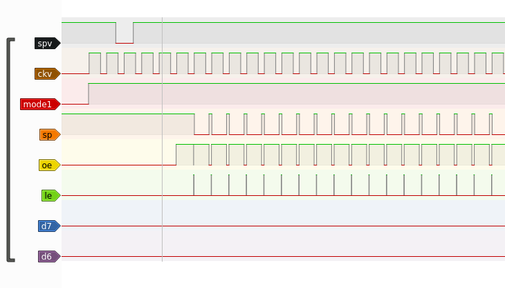
Frame signals timing:

- MODE1 high for the duration of the frame (no CKV clk is sent without MODE1 being high)
- 5 CKV pulses after mode high
  - SPV goes low during the high state of the 2nd CKV pulse
  - SPV goes high during the high state of the 3nd CKV pulse
- during the high state of 6th CKV pulse, row data start being shifted in:

(a)
  - CKV goes high
  - SPH goes low
  - row data shifted in (CKV goes low in 3/4 of the data shift)
  - SPH goes high and OE goes low
  - ~2us
  - LE goes high
  - OE goes high
  - LE goes low
  - CKV goes high
  - go to (a) for a next row or (b) at the end of a frame

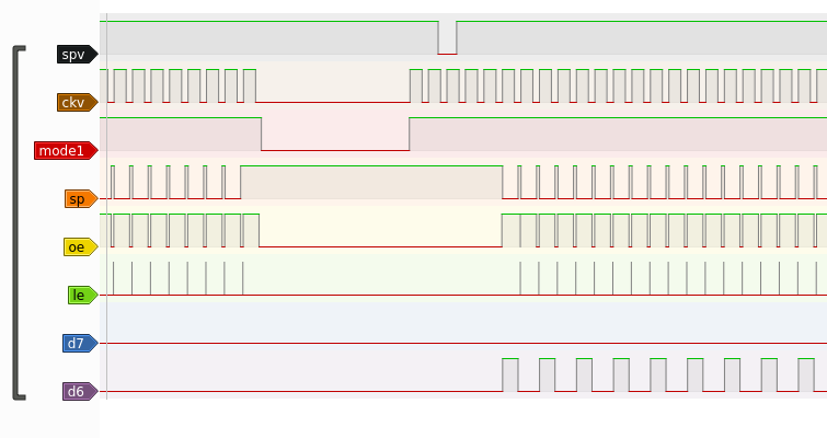
(b)
  - end of frame
  - wait for the duration of row data cycle (last row needs to be applied)
    - CKV goes low (3/4 to the end)
  - OE goes low
  - MODE1 goes low

Frame frequency can be up to 85Hz.
Frame start timings (from a logic probe):
Frame end timings:
CKH is missing, but it's just a boring 20MHz square clock signal.
Adding a serial port (voids warranty)
- UART has nice big pads on the side of the board, easy to solder some wires to
- pads are clearly marked
- 3.3V
Device disassembly
Front panel contains hooks that unlock when sticking sharp tool in between it and the back panel. Avoid bottom side of the device when opening, as it contains vulnerable cables and electronics. The back panel pops out almost too easily.
Pictures
Also known as
- PocketBook 626(2)
See also
Add some nice to have links here. This includes related devices, and external links.


