AXP152
The AXP152 is the PMIC (Power Management IC) developed by X-Powers, a sister company of Allwinner.
Overview [1]
AXP152 is a highly integrated power management IC that provides easy and flexible power solution for applications that require multi-rail outputs. It has fully met the increasingly complex needs of application processors on accurate power control.
AXP152 integrates an adaptive and USB-compatible PWM charger, four step-down converters (Buck DC-DC converter), seven low dropout regulators. It also Featuress protection circuitry such as over/under-voltage protection (OVP/UVP), over-temperature protection, and over-current protection (OCP) to guarantee the power system security and stability.
In addition, AXP152 includes a Two Wire Serial Interface (TWSI), through which the application processor is capable of enabling/disabling some power outputs, programming the voltage to decrease the power consumption, and provides customers with unprecedented experience of power management.
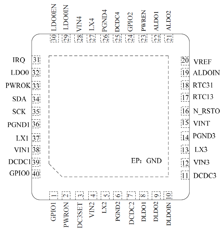
AXP152 is available in an 5mm x 5mm 40-pin QFN package.
Pinout Diagram
Features [1]
- 4*Buck DC-DC Converters
- DC-DC1:PFM/PWM mode,scaling in 1.7-3.5V,50mV/step,Output current 1A
- DC-DC2:PFM/PWM mode,scaling in 0.7-2.275V,25mV/step,Output current 2A, DVM
- DC-DC3:PFM/PWM mode,scaling in 1.7-3.5V,50mV/step,Output current 1.2A
- DC-DC4:PFM/PWM mode,scaling in 1.7-3.5V,25mV/step,Output current 1.2A
- System Management
- Support software shutdown or hardware power off
- External wakeup source
- Output monitor
- PWROK signal for reset or power off
- OVP/UVP
- Programable power on voltage or sequence
- 7 LDOs
- LDO0:Output current 1.5A,Internal 500/900/1500mA current limited option
- RTCLDO:On for RTC31,Output 3.1V, One for RTC13,Output 1.3/1.8V
- ALDO1:Analog LDO,scaling in 1.2-3.3V, 300mA
- ALDO2:Analog LDO,scaling in 1.2-3.3V, 300mA
- DLDO1:Digtal LDO or Switch,scaling in 0.7-3.5V,100mV/step,300mA
- DLDO2:Digtal LDO or Switch,scaling in 0.7-3.5V,100mV/step,300mA
- GPIOLDO:Low noise LDO, scaling in 0.7-3.5V,100mV/step,30mA
- Host Interface
- Programable Interrupt and wakeup management
- Multi-function Pins
- Internal Timer
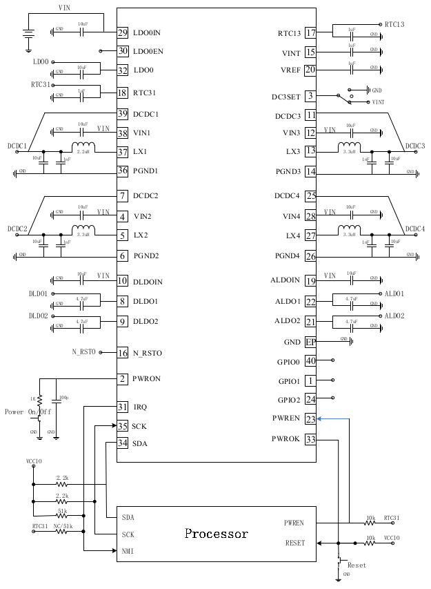
Typical Usage
AXP 152 usage with single or no battery
AXP 152 usage with another PMU (usually with multi-cell battery)
Pinout List
| Number | Pin Name | Type | Control Criteria | Description |
|---|---|---|---|---|
| 1 | GPIO1 | IO | Reg 91h [2:0] | GPIO1 |
| 2 | PWRON | I | Power On-Off key (PEK) input, Internal 100kΩ pull-up resistor to APS | |
| 3 | DC3SET | I | Set the default output voltage for DC-DC3 | |
| 4 | VIN2 | PI | DC-DC2 Input Source | |
| 5 | LX2 | IO | DC-DC2 Inductor | |
| 6 | PGND2 | G | DC-DC2 NMOS ground | |
| 7 | DCDC2 | I | DC-DC2 Feedback | |
| 8 | DLDO1 | O | DLDO1 Output | |
| 9 | DLDO2 | O | DLDO2 Output | |
| 10 | DLDOIN | PI | DLDO Input Source | |
| 11 | DCDC3 | I | DC-DC3 Feedback | |
| 12 | VIN3 | PI | DC-DC3 Input Source | |
| 13 | LX3 | IO | DC-DC3 Inductor | |
| 14 | PGND3 | G | DC-DC3 NMOS ground | |
| 15 | VINT | PO | Internal logic power, 2.5V | |
| 16 | N_RSTO | O | Output enable signal for external power module | |
| 17 | RTC13 | O | RTC power output for host RTC block | |
| 18 | RTC31 | IO | RTC power output or input for host RTC block | |
| 19 | ALDOIN | PI | Power supply for analog and ALDO1/2 | |
| 20 | VREF | I | Internal reference voltage | |
| 21 | ALDO2 | O | ALDO2 Output | |
| 22 | ALDO1 | O | ALDO1 Output | |
| 23 | PWREN | IO | Reg 93h [2:0] | Enable input for some power module, can be configured for GPIO3 (REG93 [3:0]) |
| 24 | GPIO2 | IO | Reg 92h [2:0] | GPIO2 / SYSEN |
| 25 | DCDC4 | I | DC-DC4 Feedback | |
| 26 | PGND4 | G | DC-DC4 NMOS ground | |
| 27 | LX4 | IO | DC-DC4 Inductor | |
| 28 | VIN4 | PI | DC-DC4 Input Source | |
| 29 | LDO0IN | PI | LDO0 Input Source | |
| 30 | LDO0EN | I | LDO0 Enable Input | |
| 31 | IRQ | IO | IRQ output | |
| 32 | LDO0 | PO | LDO0 Output | |
| 33 | PWROK | O | Power good indicator | |
| 34 | SDA | IO | Serial interface data pin. Normally pulled-up to 3.3V by 2.2k resistor | |
| 35 | SCK | I | Serial interface clock pin. Normally pulled-up to 3.3V by 2.2k resistor | |
| 36 | PGND1 | G | DC-DC1 NMOS ground | |
| 37 | LX1 | IO | DC-DC1 Inductor | |
| 38 | VIN1 | PI | DC-DC1 Input Source | |
| 39 | DCDC1 | I | DC-DC1 Feedback | |
| 40 | GPIO0 | IO | Reg 90h [2:0] | GPIO0 |
| 41 | EP (GND) | G | Exposed Pad, need to connect to ground |
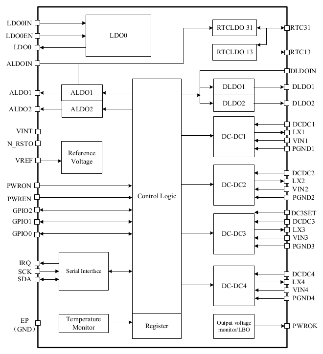
Functional Diagram
Control and Operation
Regulators
This section corresponds to section 9.2 in the datasheet.
The AXP152 features 4 DC-DC step-down (buck) converters, and 7 linear regulators. The DC-DC converters operate in automatic (PFM + PWM) or PWM mode, controllable via reg 80h, at a default frequency of 2.25 MHz. The frequency is controlled via reg 37h. It also supports spread spectrum.
| Output | Type | Voltage Range | Default Voltage | Enable steps | Example Usage | Maximum Output | Note |
|---|---|---|---|---|---|---|---|
| DCDC1 | Buck | 1.7 - 3.5 V | Configurable | 1 | 3.3V I/O | 1000 mA | |
| DCDC2 | Buck | 0.7 - 2.275 V | Configurable | 1 | 1.25V core | 2000 mA | |
| DCDC3 | Buck | 0.7 - 3.5 V | Configurable | 1 | 1.5V DDR | 1200 mA | |
| DCDC4 | Buck | 0.7 - 3.5 V | Configurable | 1 | 1.25V CPU | 1200 mA | |
| RTC-LDO | LDO | Fixed | 3.1/1.3/1.8 V | 1 | RTC | 30 mA | Always on |
| LDO0 | LDO | 0.7 - 3.3 V | Off | Off | N/A | 1500 mA | Can be used for current limiting |
| ALDO1 | LDO | 0.7 - 3.3 V | Off | Off | N/A | 300 mA | Low noise |
| ALDO2 | LDO | 0.7 - 3.3 V | 1.8 V | 1 | N/A | 300 mA | Low noise |
| DLDO1 | LDO | 0.7 - 3.3 V | Off | Off | N/A | 300 mA | |
| DLDO2 | LDO | 0.7 - 3.3 V | Off | Off | N/A | 300 mA | |
| LDOIO0 | LDO | 0.7 - 3.3 V | Off | Off | N/A | 20 mA | Low noise, output on GPIO0 |
Interrupts
This section corresponds to section 9.6 in the datasheet.
The AXP221 pulls the IRQ pin low to signal an interrupt to the host, and stores the interrupt status in the interrupt status registers (48h ~ 4Ch). Writing 1 to the corresponding bit clears the interrupt. When there are no interrupts, the IRQ pin is pulled up (by an external 51KΩ resistor). Each interrupt can be masked via the interrupt control registers (40h ~ 44h).
| Register Address | |||||
|---|---|---|---|---|---|
| Control | Status | Bit | Interrupt # | Description | Notes |
| 40h | 48h | [7] | |||
| 40h | 48h | [6] | IRQ 1 | LDO0IN connected | |
| 40h | 48h | [5] | IRQ 2 | LDO0IN removed | |
| 40h | 48h | [4] | |||
| 40h | 48h | [3] | IRQ 3 | ALDO0IN connected | |
| 40h | 48h | [2] | IRQ 4 | ALDO0IN removed | |
| 40h | 48h | [1] | |||
| 40h | 48h | [0] | |||
| 41h | 49h | [7] | |||
| 41h | 49h | [6] | |||
| 41h | 49h | [5] | IRQ 5 | DC-DC1 output voltage lower than 90% | |
| 41h | 49h | [4] | IRQ 6 | DC-DC2 output voltage lower than 90% | |
| 41h | 49h | [3] | IRQ 7 | DC-DC3 output voltage lower than 90% | |
| 41h | 49h | [2] | IRQ 8 | DC-DC4 output voltage lower than 90% | |
| 41h | 49h | [1] | IRQ 9 | PEK short press | See reg 36h |
| 41h | 49h | [0] | IRQ 10 | PEK long press | See reg 36h |
| 42h | 4Ah | [7] | IRQ 11 | Timer expired | See reg 8Ah |
| 42h | 4Ah | [6] | IRQ 12 | PEK rising edge | |
| 42h | 4Ah | [5] | IRQ 13 | PEK falling edge | |
| 42h | 4Ah | [4] | |||
| 42h | 4Ah | [3] | IRQ 14 | GPIO 0 edge trigger | See reg 90h |
| 42h | 4Ah | [2] | IRQ 15 | GPIO 1 edge trigger | See reg 91h |
| 42h | 4Ah | [1] | IRQ 16 | GPIO 2 (SYSEN) edge trigger | See reg 92h |
| 42h | 4Ah | [0] | IRQ 17 | GPIO 3 (PWREN) edge trigger | See reg 93h |
Registers
Power Control
REG 01H: Power operating mode and charge status indication
Bit Description R/W 7-6 Reserved R 5 LDO0IN status when LDO0EN pin is high 0: LDO0IN not present (< 3.5V); 1: LDO0IN present (> 3.8V)
R 4 TWI interface enabled (SIEN pin) R 3 IRQ pin triggered power on R 2 PWRON button triggered power on R 1 Reserved R 0 ALDOIN rising edge triggered power on R
REG 12H: Power output control
Bit Description R/W Default Value 7 DC-DC1 on/off RW OTP 6 DC-DC2 on/off RW OTP 5 DC-DC3 on/off RW OTP 4 DC-DC4 on/off RW OTP 3 ALDO1 on/off RW OTP 2 ALDO2 on/off RW OTP 1 DLDO1 on/off RW OTP 0 DLDO2 on/off RW OTP
REG 13H: ALDO1/2 operation mode control
Bit Description R/W Default Value 7-4 none 3 ALDO1 operation mode 0: low noise; 1: low power
RW 0 2 ALDO2 operation mode 0: low noise; 1: low power
RW 0 1-0 Reserved RW 00
REG 15H: LDO0 control
Bit Description R/W Default Value 7 LDO0 on/off no effect if LDO0EN is connected to LDO0IN
RW 0 6 Reserved RW 0 5-4 LDO0 voltage 00: 5V ; 01: 3.3V 10: 2.8V ; 11: 2.5V
RW 00 3-2 Reserved RW 00 1-0 LDO0 current limit 00: no limit 01: 1500mA 10: 900mA 11: 500mA
RW 00
Reg 23h: DC-DC2 output voltage
Bit Description R/W Default Value 7-6 Reserved 5-0 0.7 - 2.275 V, 25 mV/step RW OTP
Reg 25h: DC-DC 2 Voltage Ramp Control
Bit Description R/W Default Value 7-4 None 3 Reserved RW 0 2 DC-DC2 VRC enable RW 0 1 Reserved RW 0 0 DC-DC2 voltage ramp rate 0: 25mV/15.625μs = 1.6mV/μs 1: 25mV/31.250μs = 0.8mV/μs
RW 0
Reg 26h: DC-DC1 output voltage
Bit Description R/W Default Value 7-4 None 3-0 0000: 1.7V 0001: 1.8V 0010: 1.9V 0011: 2.0V 0100: 2.1V 0101: 2.4V 0110: 2.5V 0111: 2.6V 1000: 2.7V 1001: 2.8V 1010: 3.0V 1011: 3.1V 1100: 3.2V 1101: 3.3V 1110: 3.4V 1111: 3.5V
RW OTP
Reg 27h: DC-DC3 output voltage
Bit Description R/W Default Value 7-6 Reserved RW 00 5-0 0.7 - 3.5 V, 50 mV/step RW OTP & DC3SET pin
Reg 28h: ALDO1/2 output voltage
Bit Description R/W Default Value 7-4 ALDO1 output voltage 0000: 1.2V 0001: 1.3V 0010: 1.4V 0011: 1.5V 0100: 1.6V 0101: 1.7V 0110: 1.8V 0111: 1.9V 1000: 2.0V 1001: 2.5V 1010: 2.7V 1011: 2.8V 1100: 3.0V 1101: 3.1V 1110: 3.2V 1111: 3.3V
RW OTP 3-0 ALDO2 output voltage 0000: 1.2V 0001: 1.3V 0010: 1.4V 0011: 1.5V 0100: 1.6V 0101: 1.7V 0110: 1.8V 0111: 1.9V 1000: 2.0V 1001: 2.5V 1010: 2.7V 1011: 2.8V 1100: 3.0V 1101: 3.1V 1110: 3.2V 1111: 3.3V
RW OTP
Reg 29h: DLDO1 voltage control
Bit Description R/W Default Value 7 DLDO1 mode 0: LDO mode, voltage controlled by bits [4:0] 1: Switch mode, voltage close to DLDOIN
RW 0 6-5 Reserved RW 00 4-0 0.7 - 3.3 V, 100 mV/step RW OTP
Reg 2Ah: DLDO2 voltage control
Bit Description R/W Default Value 7 DLDO2 mode 0: LDO mode, voltage controlled by bits [4:0] 1: Switch mode, voltage close to DLDOIN
RW 0 6-5 Reserved RW 00 4-0 0.7 - 3.3 V, 100 mV/step RW OTP
Reg 2Bh: DC-DC4 output voltage
Bit Description R/W Default Value 7 Reserved RW 0 6-0 0.7 - 3.5 V, 25 mV/step RW OTP
Reg 31h: Power recovery and VOFF control
Bit Description R/W Default Value 7 Pull down PWROK when power recovers 0: Don't pull down PWROK 1: Pull down PWROK during wakeup
RW 0 6-4 Reserved RW 000 3 Power recovery enable 0: Not enabled; 1: Enabled; Auto-cleared
RW 0 2-0 VOFF voltage: 2.6 - 3.3V, 100 mV/step
RW 111
REG 32h: Shutdown control
Bit Description R/W Default Value 7 Shutdown; Writing 1 turns off AXP152; auto-cleared RW 0 6-3 Reserved RW 0000 2 Output power off sequence 0: Turn off all outputs at the same time 1: Reverse of power on sequence
RW 0 1-0 Reserved RW 00
REG 36h: PEK button parameters
Bit Description R/W Default Value 7-6 Power on timing 00: 128ms; 01: 3s; 10: 1s; 11: 2s
RW 10 5-4 Long press timing T = [ 1 + (bit 1-0) * 0.5 ] S; default: 1.5S RW 01 3 Automatic shutdown when pressed longer than Tshutdown RW 1 2 PWROK delay after power on 0: 8ms ; 1: 64ms
RW 1 1-0 Tshutdown = [ 4 + (bit 1-0) * 2 ] s; default: 6s RW 01
Reg 37h: DC-DC operating frequency
Default value: 08h
| Bit | Description | R/W | Default Value |
|---|---|---|---|
| 7 | Enable spread spectrum for DC-DC | RW | 0 |
| 6 | DC-DC spread spectrum bandwidth
0: 50 KHz; 1: 100KHz |
RW | 0 |
| 5-4 | reserved | RW | 00 |
| 3-0 | DC-DC switching frequency F = [1 + / - (Bit3-0) * 5%)] * 2.25MHz | RW | 1000 |
REG 80h: DC-DC operation mode
Bit Description Value R/W Default Value 7-4 Reserved RW 0000 3 DC-DC1 operation mode 0: PFM+PWM 1: PWM
RW 0 2 DC-DC2 operation mode RW 0 1 DC-DC3 operation mode RW 0 0 DC-DC4 operation mode RW 0
GPIO controls
REG 90H: GPIO0 control
Bit Description Values R/W Default Value 7 Enable GPIO0 rising edge IRQ/wakeup 1 to enable RW 0 6 Enable GPIO0 falling edge IRQ/wakeup 1 to enable RW 0 5-3 Reserved 2-0 GPIO0 pin function 000: output low 001: output high (DC-DC1) 010: PWM0 output (DC-DC1) 011: input 1XX: floating
RW 111
REG 91H: GPIO1 control
Bit Description Values R/W Default Value 7 Enable GPIO1 rising edge IRQ/wakeup 1 to enable RW 0 6 Enable GPIO1 falling edge IRQ/wakeup 1 to enable RW 0 5-3 Reserved 2-0 GPIO1 pin function 000: output low 001: output high (DC-DC1) 010: PWM1 output (DC-DC1) 011: input 1XX: floating
RW 111
REG 92H: GPIO2 (SYSEN) control
Bit Description Values R/W Default Value 7 Enable GPIO2 rising edge IRQ/wakeup 1 to enable RW 0 6 Enable GPIO2 falling edge IRQ/wakeup 1 to enable RW 0 5-3 Reserved 2-0 GPIO1 pin function 000: output low 001: floating 010: low noise LDO 011: input 1XX: floating
RW 111
REG 93H: GPIO3 (PWREN) control
Bit Description Values R/W Default Value 7 Enable GPIO3 rising edge IRQ/wakeup 1 to enable RW 0 6 Enable GPIO3 falling edge IRQ/wakeup 1 to enable RW 0 5-3 Reserved 2 GPIO1 pin function 000: output low 001: floating 010: floating 011: input 1XX: floating
RW 111
REG 96h: GPIO2 LDO voltage control
Bit Description Values R/W Default Value 7-4 Reserved 3-0 GPIO2 LDO output voltage Vout = 1.8 + 0.1 * (Bit 3-0) V RW 1010
REG 97h: GPIO [3:0] input
Bit Description Values R/W 7-4 Reserved 3 GPIO 3 input value R 2 GPIO 2 input value R 1 GPIO 1 input value R 0 GPIO 0 input value R
REG 98h: PWM0 frequency control X0
Bit Description Values R/W 7-0 PWM0 frequency (X0) 0 ~ 255 RW
PWM0 frequency = 2.25 MHz / (X0 + 1) / Y0
REG 99h: PWM0 frequency / duty cycle control Y0
Bit Description Values R/W 7-0 PWM0 frequency / duty cycle (Y0) 0 ~ 255 RW
REG 9Ah: PWM0 duty cycle control Z0
Bit Description Values R/W 7-0 PWM0 duty cycle (Z0) 0 ~ Y0 RW
PWM0 duty cycle = Z0 / Y0
REG 9Bh: PWM1 frequency control X1
Bit Description Values R/W 7-0 PWM1 frequency (X1) 0 ~ 255 RW
PWM1 frequency = 2.25 MHz / (X1 + 1) / Y1
REG 9Ch: PWM1 frequency / duty cycle control Y0
Bit Description Values R/W 7-0 PWM1 frequency / duty cycle (Y1) 0 ~ 255 RW
REG 9Dh: PWM1 duty cycle control Z1
Bit Description Values R/W 7-0 PWM1 duty cycle (Z1) 0 ~ Y1 RW
PWM1 duty cycle = Z1 / Y1
Interrupts
See Interrupts section.
Spec Sheets
AXP152 Datasheet v1.0 (PDF, 34 pages, 2012-04-01)
See Also
References
- ↑ 1.0 1.1 X-Powers AXP152 Taken on 2014-05-26


