NFC Register Guide
NAND Flash Controller
Warning, default values where obtained using mtest in u-boot. They all kept reading 0, no matter what was written to them. So it could be write only or otherwise. Q: Could it possible that you're reading while NFC is disabled?
Overview
| regid | bit | size | access | default | desc | E |
|---|
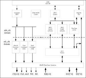
NFC Block Diagram
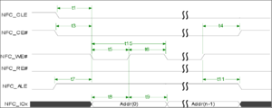
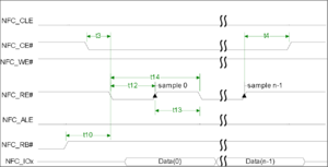
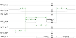
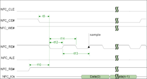
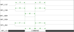
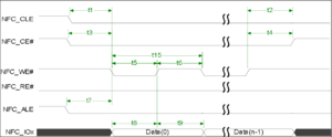
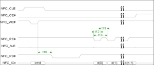
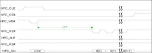
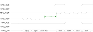
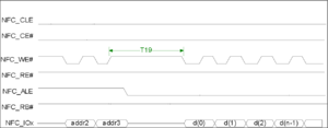
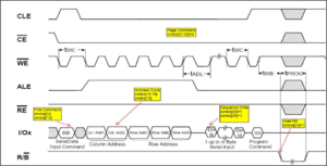
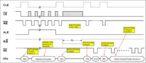
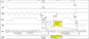
NFC Timing Diagrams
See thumbnails to the right
NFC Timing Cycle List
1T is 2x NFC_CLK.
| ID | Parameter | Timing | Notes |
|---|---|---|---|
| T1 | NFC_CLE setup time | 1T | Example |
| T2 | NFC_CLE hold time | 1T | Example |
| T3 | NFC_CE setup time | 1T | Example |
| T4 | NFC_CE hold time | 1T | Example |
| T5 | NFC_WE# pulse width | 1T | Example |
| T6 | NFC_WE# hold time | 1T | Example |
| T7 | NFC_ALE setup time | 1T | Example |
| T8 | Data setup time | 1T | Example |
| T9 | Data hold time | 1T | Example |
| T10 | Ready to NFC_RE# low | 3T | Example |
| T11 | NFC_ALE hold time | 1T | Example |
| T12 | NFC_RE# pulse width | 1T | Example |
| T13 | NFC_RE# hold time | 1T | Example |
| T14 | Read cycle time | 2T | Example |
| T15 | Write cycle time | 2T | Example |
| T16 | NFC_WE# high to R/B# busy | tWB | Specified by timing configure register(NFC_TIMING_CFG) |
| T17 | NFC_WE# high to NFC_RE# low | tWHR | Specified by timing configure register(NFC_TIMING_CFG) |
| T18 | NFC_RE# high to NFC_WE# low | tRHW | Specified by timing configure register(NFC_TIMING_CFG) |
| T19 | Address to Data Loading time | tADL | Specified by timing configure register(NFC_TIMING_CFG) |
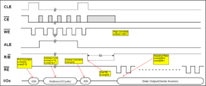
NFC Operation Guide
See thumbnails to the right.
NFC Registers
NFC Base address: 0x01c03000
| Register Name | Offset | Size | Description |
|---|---|---|---|
| NFC_CTL | 0x0000 | 4 B | NFC control |
| NFC_ST | 0x0004 | 4 B | NFC status |
| NFC_INT | 0x0008 | 4 B | NFC interrupt control |
| NFC_TIMING_CTL | 0x000c | 4 B | NFC NAND timing control |
| NFC_TIMING_CFG | 0x0010 | 4 B | NFC NAND timing configuration |
| NFC_ADDR_LOW | 0x0014 | 4 B | NFC low word of address |
| NFC_ADDR_HIGH | 0x0018 | 4 B | NFC high word of address |
| NFC_SECTOR_NUM | 0x001c | 4 B | NFC sector count |
| NFC_CNT | 0x0020 | 4 B | NFC byte count |
| NFC_CMD | 0x0024 | 4 B | NFC command |
| NFC_READ_CMD_SET | 0x0028 | 4 B | NFC set read command |
| NFC_WRITE_CMD_SET | 0x002c | 4 B | NFC set write command |
| NFC_IO_DATA | 0x0030 | 4 B | NFC I/O port |
| NFC_ECC_CTL | 0x0034 | 4 B | NFC ECC control |
| NFC_ECC_ST | 0x0038 | 4 B | NFC ECC status |
| NFC_DEBUG | 0x003c | 4 B | NFC debug |
| NFC_ECC_CNT0 | 0x0040 | 4 B | NFC ECC corrected count for block 0-3 |
| NFC_ECC_CNT1 | 0x0044 | 4 B | NFC ECC corrected count for block 4-7 |
| NFC_ECC_CNT2 | 0x0048 | 4 B | NFC ECC corrected count for block 8-11 |
| NFC_ECC_CNT3 | 0x004c | 4 B | NFC ECC corrected count for block 12-15 |
| NFC_USER_DB | 0x0050 | 64 B | NFC user data for block 0-15 |
| NFC_SPARE_AREA | 0x00a0 | 4 B | Offset of the spare area in a page |
| NFC_RAM0 | 0x0400 | 1 kiB | Base address for SRAM0 (I/O) |
| NFC_RAM1 | 0x0800 | 1 kiB | Base address for SRAM1 (I/O) |
NFC_CTL
Default value: 0x0000
Offset: 0x0000
| Name | Bit | Read/Write | Default | Values | Description |
|---|---|---|---|---|---|
| NFC_EN | 0 | Read/Write | 0b0 |
    0 = disable
    1 = enable
|
Enable or disable the NAND flash controller |
| NFC_RESET | 1 | Read/Write | 0b0 |
    When read:
    0 = reset finished
    1 = reset in progress
    when write:
    1 = start a reset progress
|
Reset the NAND flash controller |
| NFC_BUS_WIDTH | 2 | Read/Write | 0b0 |
    0 = 8 bit
    1 = 16 bit
|
NFC bus width |
| NFC_RB_SEL | 3 | Read/Write | 0b0 |
    0 = r/b pin 0
    1 = r/b pin 1
|
Selects one of the two R/B pin of NFC |
| NFC_CE_CTL0 | 6 | Read/Write | 0b0 |
? |
NFC collumn ... control 0? |
| NFC_CE_CTL1 | 7 | Read/Write | 0b0 |
? |
NFC collumn ... control 1? |
| NFC_PAGE_SIZE | 8:11 | Read/Write | 0x00 |
    0x00 = 1 kiB
    0x01 = 2 kiB
    0x02 = 4 kiB
    0x03 = 8 kiB
    0x04 = 16 kiB
|
NFC page size (page shift - 10) |
| NFC_SAM | 12 | Read/Write | 0b0 |
? |
NFC SAM |
| reserved | 13 | ||||
| NFC_RAM_METHOD | 14 | Read/Write | 0b0 |
    0 = Use SRAM for data transfer
    1 = Use DMA for data transfer
|
NFC RAM method |
| reserved | 15:17 | ||||
| DDR_TYPE | 18:19 | Read/Write | 0x00 |
    0x00, 0x01 = None DDR Type
    0x10 = ONFI DDR type
    0x11 = Toggle DDR type
|
|
| REPEAT_MODE | 20 | Read/Write | 0x0 |
0 = disable repeat mode 1 = enable repeat mode |
this bit only work under DDR mode, see bit 18:19 |
| reserved | 21:23 | ||||
| NFC_CE_SEL | 24:27 | Read/Write | 0x00 |
n = chip n |
If n=0-7, selects the CS pin on the NFC. if n=8-15, doesn't select any CS pin (can be used with GPIO pin as CS pin) |
| reserved | 28:30 | ||||
| NFC_DEBUG_CTL | 31 | Read/Write | 0b0 |
    0 = disable
    1 = enable
|
NFC debug control |
NFC_ST
Default value: 0x00000f00
Offset: 0x0004
| Name | Bit | Read/Write | Default | Values | Description |
|---|---|---|---|---|---|
| NFC_RB_B2R | 0 | Read/Write | 0b0 |
Read: 1 = Transition from Busy to Ready Write: 1 = Clear the flag |
NFC R/B Busy-to-Ready interrupt flag |
| NFC_CMD_INT_FLAG | 1 | Read/Write | 0b0 |
Read: 0 = Command pending 1 = Command completed Write: 1 = Clear the flag If any error occurs, this flag will stay 0 |
NFC command interrupt flag |
| NFC_DMA_INT_FLAG | 2 | Read/Write | 0b0 |
Read: 0 = DMA pending 1 = DMA completed Write: 1 = Clear the flag |
NFC DMA interrupt flag |
| NFC_CMD_FIFO_STAT | 3 | Read/Write | 0b0 |
0 = Command FIFO can receive new command 1 = Command FIFO is full |
NFC command FIFO status |
| NFC_STAT | 4 | Read/Write | 0b0 |
    0 = ?
    1 = ?
|
NFC status |
| NFC_MATCH_INT_FLAG | 5 | Read/Write | 0b0 |
    0 = ?
    1 = ?
|
NFC command dma flag |
| reserved | 6:7 | ||||
| NFC_RB_STATE0 | 8 | Read/Write | 0b1 |
0 = NAND busy 1 = NAND ready |
NFC R/B state for line 0 |
| NFC_RB_STATE1 | 9 | Read/Write | 0b1 |
0 = NAND busy 1 = NAND ready |
NFC R/B state for line 1 |
| NFC_RB_STATE2 | 10 | Read/Write | 0b1 |
0 = NAND busy 1 = NAND ready |
NFC R/B state for line 2 |
| NFC_RB_STATE3 | 11 | Read/Write | 0b1 |
0 = NAND busy 1 = NAND ready |
NFC R/B state for line 3 |
| reserved | 12:31 | 0x00 |
NFC_INT
Default value: 0x0000
Offset: 0x0008
| Name | Bit | Read/Write | Default | Values | Description |
|---|---|---|---|---|---|
| NFC_B2R_INT_EN | 0 | Read/Write | 0b0 |
    0 = Disable
    1 = Enable
|
NFC R/B Busy-to-Ready interrupt enable |
| NFC_CMD_INT_EN | 1 | Read/Write | 0b0 |
    0 = Disable
    1 = Enable
|
NFC command interrupt enable |
| NFC_DMA_INT_EN | 2 | Read/Write | 0b0 |
    0 = Disable
    1 = Enable
|
NFC DMA interrupt enable |
| reserved | 3:31 | 0x00 |
NFC_TIMING_CTL
Default value: 0x0000
| Name | Bit | Read/Write | Default | Values | Description |
|---|---|---|---|---|---|
| NFC_DC_CTL | 0:5 | Read/Write | 0x00 |
? |
NFC delay chain control |
| reserved | 6:7 | 0x00 | |||
| NFC_READ_PIPE | 8:11 | Read/Write | 0x00 |
? |
NFC read pipe? |
| reserved | 12:31 | 0x00 |
NFC_CMD
Default value: 0x0000
Offset: 0x0024
| Name | Bit | Read/Write | Default | Values | Description |
|---|---|---|---|---|---|
| NFC_CMD_LOW | 0:7 | Read/Write | 0x00 |
? |
NFC low byte command |
| NFC_CMD_HIGH | 8:15 | Read/Write | 0x00 |
? |
NFC high byte command |
| NFC_ADDR_NUM | 16:18 | Read/Write | 0x00 |
address number - 1 |
NFC address number |
| NFC_SEND_ADDR | 19 | Read/Write | 0b0 |
    0 = not have address cycle
    1 = have address cycle
|
NFC send address |
| NFC_XS_DIR | 20 | Read/Write | 0b0 |
    0 = fetch data from flash chip
    1 = send data to flash chip
|
NFC access direction |
| NFC_DATA_TRANS | 21 | Read/Write | 0b0 |
    0 = do not fetch data to NFC RAM
    1 = fetch data to NFC RAM
|
NFC data transfer |
| NFC_SEND_CMD0 | 22 | Read/Write | 0b0 |
? |
NFC send command 0 |
| NFC_WAIT_FLAG | 23 | Read/Write | 0b0 |
    0 = not wait r/b ready
    1 = wait r/b ready
|
NFC wait flag |
| NFC_SEND_CMD1 | 24 | Read/Write | 0b0 |
? |
NFC send command 1 |
| NFC_SEQ | 25 | Read/Write | 0b0 |
? |
NFC sequence? |
| NFC_DATA_SWAP_METHOD | 26 | Read/Write | 0b0 |
? |
NFC data swap method |
| NFC_ROW_AUTO_INC | 27 | Read/Write | 0b0 |
? |
NFC row auto increase |
| NFC_SEND_CMD2 | 28 | Read/Write | 0b0 |
? |
NFC send command 2 |
| NFC_SEND_CMD3 | 29 | Read/Write | 0b0 |
? |
NFC send command 3 |
| NFC_CMD_TYPE | 30:31 | Read/Write | 0b00 |
? |
NFC command type |
NFC_READ_CMD_SET
Default value: 0x00e00f30
Offset: 0x0028
| Name | Bit | Read/Write | Default | Values | Description |
|---|---|---|---|---|---|
| NFC_READ_CMD | 0:7 | Read/Write | 0x30 |
? |
NFC read command |
| NFC_RANDOM_READ_CMD0 | 8:15 | Read/Write | 0x05 |
? |
NFC random read command 0 |
| NFC_RANDOM_READ_CMD1 | 16:23 | Read/Write | 0xe0 |
? |
NFC random read command 1 |
| reserved | 24:31 | 0x00 |
NFC_WRITE_CMD_SET
Default value: 0x70008510
Offset: 0x002c
| Name | Bit | Read/Write | Default | Values | Description |
|---|---|---|---|---|---|
| NFC_PROG_CMD | 0:7 | Read/Write | 0x10 |
? |
NFC program command |
| NFC_RANDOM_WRITE_CMD | 8:15 | Read/Write | 0x85 |
? |
NFC random write command |
| NFC_READ_CMD0 | 16:23 | Read/Write | 0x00 |
? |
NFC read command 0 |
| NFC_READ_CMD1 | 24:31 | Read/Write | 0xe0 |
? |
NFC read command 1 |
NFC_ECC_CTL
Default value: 0x4a800008
Offset: 0x0034
| Name | Bit | Read/Write | Default | Values | Description |
|---|---|---|---|---|---|
| NFC_ECC | 0 | Read/Write | 0b0 |
    0 = disable
    1 = enable
|
NFC ECC enable or disable |
| reserved | 1:2 | 0x00 | |||
| NFC_ECC_PIPELINE | 3 | Read/Write | 0b0 |
0= disable ecc pipeline 1= enable ecc pipeline |
NFC ECC pipeline enable/disable |
| NFC_ECC_EXCEPTION | 4 | Read/Write | 0b1 |
      0 = disable Ecc exception
      1=enable
|
NFC ECC exception enable/disable |
| NFC_ECC_BLOCK_SIZE | 5 | Read/Write | 0b0 |
? |
NFC ECC block size |
| reserved | 6:8 | 0x00 | |||
| NFC_ECC_RANDOM | 9 | Read/Write | 0b0 |
    0 = disabled
    1 = enabled
|
NFC random ecc enable/disable |
| NFC_ECC_RANDOM_DIR | 10 | Read/Write | 0b0 |
? |
NFC random ecc direction |
| reserved | 11 | 0b0 | |||
| NFC_ECC_MODE | 12:15 | Read/Write | 0x00 |
0 = 16bit 1 = 24bit 2 = 28bit 3 = 32bit 4 = 40bit 5 = 48bit 6 = 56bit 7 = 60bit 8 = 64bit |
ECC can correct how many bits for amount of NFC_REG_CNT data |
| NFC_ECC_RANDOM_SEED | 16:31 | Read/Write | 0x4a80 |
16 bit value |
NFC ecc random seed[1] |
- ↑ See Random Seed
NFC_USER_DB
Default value: 0xff * 64
Offset: 0x0050
| Name | Bit | Read/Write | Default | Values | Description |
|---|---|---|---|---|---|
| NFC_USER_DB0 | 0:2048 | Read/Write | 0xffffffff * 64 |
64 x 32 bit value |
ECC/OOB user data area. 32 bits per sector. |
Initial values
default map
md 0x01c03000 0x29
01c03000: 00000000 00000f00 00000000 00000000    ................
01c03010: 00000095 00000000 00000000 00000000    ................
01c03020: 00000000 00000000 00e00530 70008510    ........0......p
01c03030: 00000000 4a800008 00000000 00000000    .......J........
01c03040: 00000000 00000000 00000000 00000000    ................
01c03050: ffffffff ffffffff ffffffff ffffffff    ................
01c03060: ffffffff ffffffff ffffffff ffffffff    ................
01c03070: ffffffff ffffffff ffffffff ffffffff    ................
01c03080: ffffffff ffffffff ffffffff ffffffff    ................
01c03090: 00000000 00000000 00000000 00000000    ................
01c030a0: 00000400    ....
all set to 1
mw 0x01c03000 0xffffffff 0x29 md 0x01c03000 0x29
01c03000: 0f3fcf5f 00000f00 00000007 00000f3f    _.?.........?...
01c03010: 000007ff ffffffff ffffffff 0000001f    ................
01c03020: 000003ff ffff00ff 00ffffff ffffffff    ................
01c03030: 00000000 7ffffe39 00000000 0000017f    ....9...........
01c03040: 00000000 00000000 00000000 00000000    ................
01c03050: ffffffff ffffffff ffffffff ffffffff    ................
01c03060: ffffffff ffffffff ffffffff ffffffff    ................
01c03070: ffffffff ffffffff ffffffff ffffffff    ................
01c03080: ffffffff ffffffff ffffffff ffffffff    ................
01c03090: 00000000 00000000 00000000 00000000    ................
01c030a0: 0000ffff    ....
all set to 0
mw 0x01c03000 0x00 0x29 md 0x01c03000 0x29
01c03000: 00000000 00000f00 00000000 00000000    ................
01c03010: 00000095 00000000 00000000 00000000    ................
01c03020: 00000000 00000000 00e00530 70008510    ........0......p
01c03030: 00000000 4a800008 00000000 00000000    .......J........
01c03040: 00000000 00000000 00000000 00000000    ................
01c03050: ffffffff ffffffff ffffffff ffffffff    ................
01c03060: ffffffff ffffffff ffffffff ffffffff    ................
01c03070: ffffffff ffffffff ffffffff ffffffff    ................
01c03080: ffffffff ffffffff ffffffff ffffffff    ................
01c03090: 00000000 00000000 00000000 00000000    ................
01c030a0: 00000400    ....
Hardware ECC
Spare area
Each page data write will cause a spare area data write if hardware ECC is enabled. Sometimes the page is more than 1K, so it needs multiple times to write a page. The spare area will also be written with ECC data muliple times sequencely. One time a data write op will write 4 Byte user data stored at NFC_USER_DATA(i) following ECC data whose length depending on the ECC mode.
Random Seed
The controller includes a randomizer that scrambles the data to avoid large islands of the same charge. During boot the randomizer is initialized by the BROM to 0x4a80 and thus the SPL is expected to be randomized as such. Currently, boot[01] and stock kernels use the following randomized values, it is formed by page number % 128 index into
static const unsigned short random_seed[128] = {
    0x2b75, 0x0bd0, 0x5ca3, 0x62d1, 0x1c93, 0x07e9, 0x2162, 0x3a72, 0x0d67, 0x67f9,
    0x1be7, 0x077d, 0x032f, 0x0dac, 0x2716, 0x2436, 0x7922, 0x1510, 0x3860, 0x5287,
    0x480f, 0x4252, 0x1789, 0x5a2d, 0x2a49, 0x5e10, 0x437f, 0x4b4e, 0x2f45, 0x216e,
    0x5cb7, 0x7130, 0x2a3f, 0x60e4, 0x4dc9, 0x0ef0, 0x0f52, 0x1bb9, 0x6211, 0x7a56,
    0x226d, 0x4ea7, 0x6f36, 0x3692, 0x38bf, 0x0c62, 0x05eb, 0x4c55, 0x60f4, 0x728c,
    0x3b6f, 0x2037, 0x7f69, 0x0936, 0x651a, 0x4ceb, 0x6218, 0x79f3, 0x383f, 0x18d9,
    0x4f05, 0x5c82, 0x2912, 0x6f17, 0x6856, 0x5938, 0x1007, 0x61ab, 0x3e7f, 0x57c2,
    0x542f, 0x4f62, 0x7454, 0x2eac, 0x7739, 0x42d4, 0x2f90, 0x435a, 0x2e52, 0x2064,
    0x637c, 0x66ad, 0x2c90, 0x0bad, 0x759c, 0x0029, 0x0986, 0x7126, 0x1ca7, 0x1605,
    0x386a, 0x27f5, 0x1380, 0x6d75, 0x24c3, 0x0f8e, 0x2b7a, 0x1418, 0x1fd1, 0x7dc1,
    0x2d8e, 0x43af, 0x2267, 0x7da3, 0x4e3d, 0x1338, 0x50db, 0x454d, 0x764d, 0x40a3,
    0x42e6, 0x262b, 0x2d2e, 0x1aea, 0x2e17, 0x173d, 0x3a6e, 0x71bf, 0x25f9, 0x0a5d,
    0x7c57, 0x0fbe, 0x46ce, 0x4939, 0x6b17, 0x37bb, 0x3e91, 0x76db
};
